People leave useful things out on the curb all the time. Toaster ovens. Kid’s shoes. Sofas. Old TVs. Not-so-old TVs. And, often, printers. Inkjet printers, in particular, are a rich source of important nutrients such as motors, gears, sensors, wifi, and power supplies. It’s always fun to pop them open and salvage the good stuff.
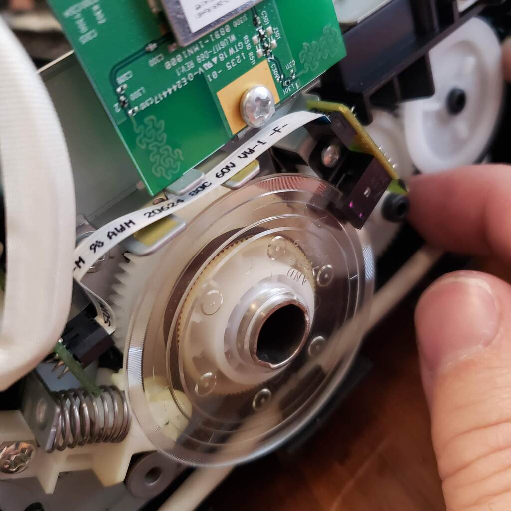
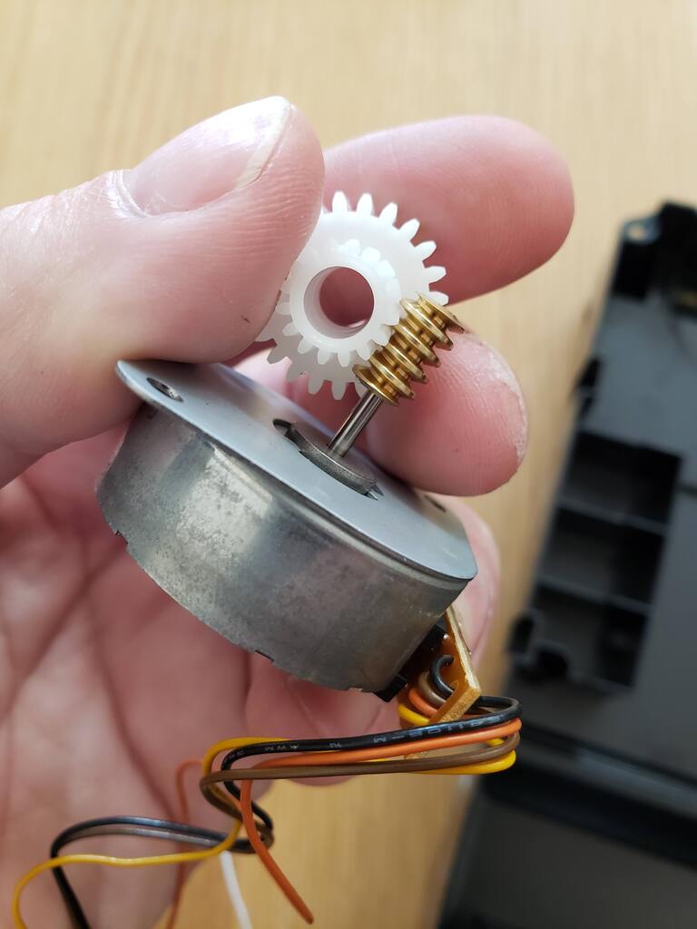
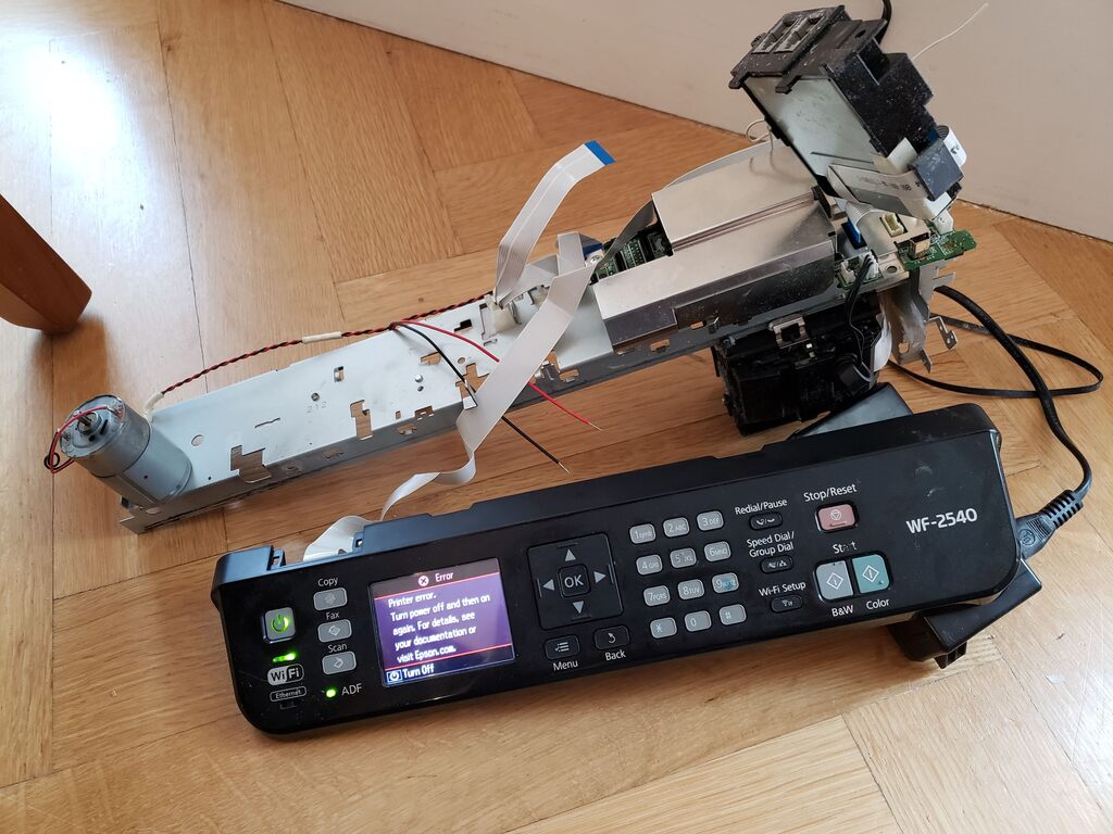
These are parts from an Epson WF-2540 I found in the trash that I spent a morning disassembling with my kids. Look at this beautiful quadrature encoder wheel. And that lovely little stepper and worm gear! There’s even a peristaltic pump in this one. It’s a bonanza. Every time I disassemble a printer, I end up with three piles: one of useful parts, one of plastic and metal scrap for recycling, and one of components that are too specific to make use of. Oh, and one of these frickin’ things:
Oh. You again.
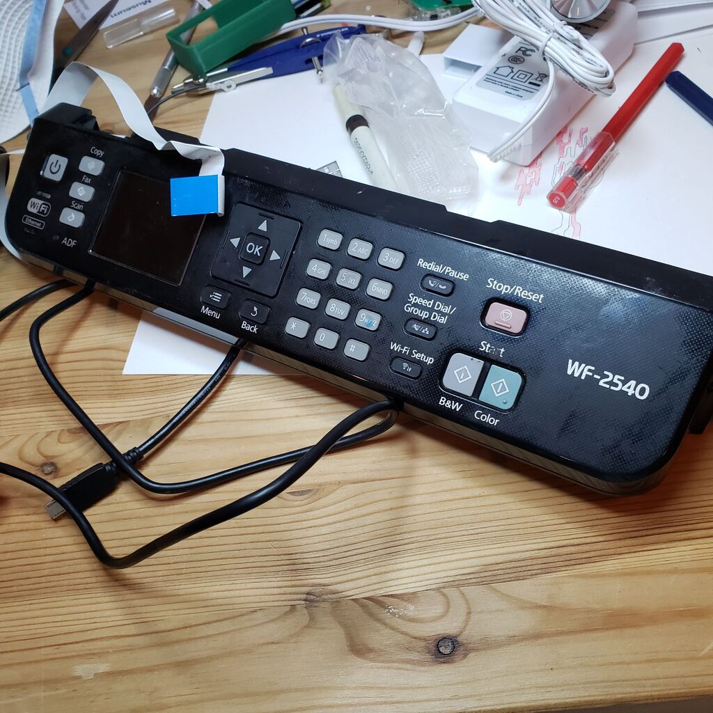
My old nemesis, the control panel. A couple dozen buttons, a few LEDs, and a color LCD, all in a well-designed, sturdy package. I can think of a half-dozen uses in a heartbeat. Wouldn’t it be nice to use this as an interface for a media player? A robot arm? A pen plotter? Your air conditioner? A midi sequencer? An overly complex toaster?
The problem is that every control panel is its own reverse engineering project. Usually I just give up on these as being too complex to reuse as a single unit, but for some reason I thought this time, I’d give it a whirl. After all, that flat cable coming out the back only has fourteen pins. How hard can it be?
I approached this project in two stages. The first was to be able to read all the keypresses and blink the LEDs, which I was pretty confident I could handle. The second, being able to display images on the embedded LCD, was, well, trickier. But let’s see how far we can get!
Figuring out the buttons and LEDs
A few screws hold together the enclosure; it comes apart pretty easily.
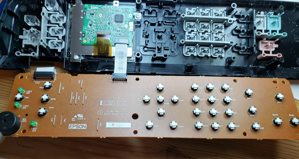
Inside there are two PCBs. The larger one is single-sided and carries the buttons and the LEDs, and the other is a small LCD controller board. There’s a ten-pin flat cable connecting the two PCBs. There’s also a little piezoelectric buzzer in the lower left corner, in case we need to make any blooping noises.
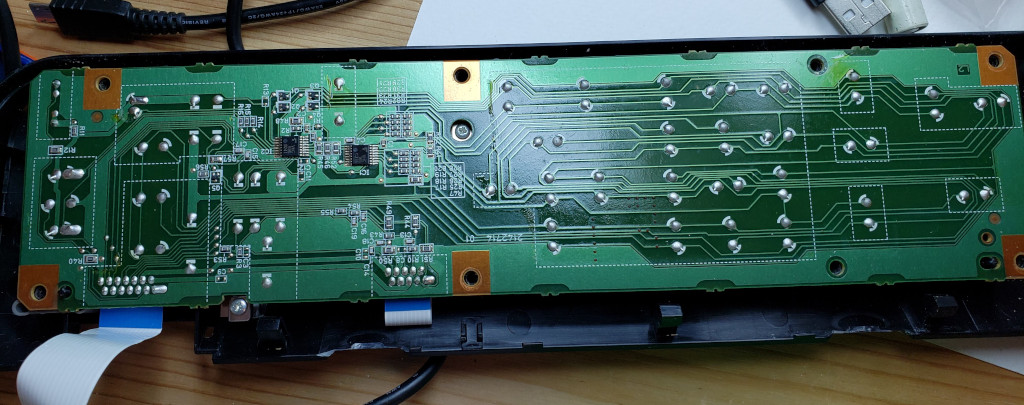
Like most keypads, this one is logically arranged as a grid. There are 28 buttons in the grid– the power button has its own dedicated line to wake up the CPU– and they’re arranged as four columns of seven rows. If the main board accessed this grid directly, it would require thirteen pins just to scan the buttons. That’s a lot, so there are a couple of ICs on the board to help reduce the number of connections and I/O pins needed.
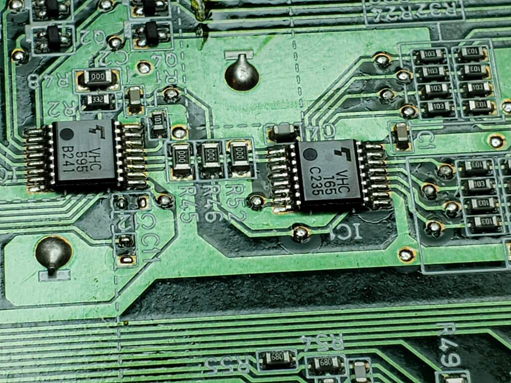
Although chip manufacturers no longer bother to mark the “74” prefix on the packages, these are 7400-series logic chips, a family of ICs that have remained essentially unchanged for half a century. The ‘165 is an 8-bit parallel-in serial-out shift register, which reads in a whole column of buttons at once when the LOAD pin goes low, and then outputs the bits one at a time when it receives a clock pulse. The ‘595 works in reverse, loading an internal shift register bit by bit on a clock pulse, and copying those bits to its output pins when there’s a positive pulse on its RCLK pin. This board wires the clock pins of both chips together, along with their LOAD/RCLK pins, so the controller can read the ‘165 to scan one row of buttons while loading the ‘595 with a new bit pattern at the same time. The outputs on the ‘595 that aren’t used to scan the grid instead power individual LEDs, so we’re controlling everything but the LCD with just four pins. (Five, if you count the output enable on the ‘595, which is routed to the connector but isn’t actually necessary and can be tied low.)
I poked around a bit with a multimeter to work out which pins on the flat cable connected to the signals I was interested in. Many of the signals are also tied to pins on the 10-pin LCD connector, so I started recording those correspondences, too. This step was also where I identified the ground and 3.3V power pins.
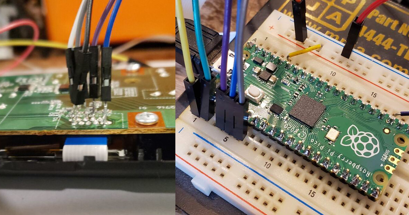
As I’m neither patient or nor diligent enough to trace out the circuit to figure out which buttons are wired up to which rows and columns, I wired up a Raspberry Pi Pico to continually scan the button grid and report the row and column location of any button presses. Then I was able to mash the keys until I figured out where everything was.
const uint8_t keymap[KB_ROWS][KB_COLS] = {
  { KEY_9,      KEY_2,      KEY_REDIAL, KEY_5,
    KEY_MENU,   KEY_0,      KEY_DOWN,   KEY_LEFT,   },
  { KEY_SCAN,   KEY_STOP,   KEY_3,      KEY_7,
    0,          KEY_HASH,   KEY_SDGD,   KEY_8,      },
  { KEY_FAX,    KEY_1,      KEY_OK,     KEY_RIGHT,
    KEY_STAR,   KEY_BW,     KEY_COLOR,  0,          },
  { KEY_COPY,   KEY_UP,     KEY_6,      KEY_4,
    KEY_BACK,   KEY_WIFI,   0,          0,          },
};
And that’s it for the buttons. There was a bit more fooling around to get the LEDs displaying what I wanted, but the keypad and LEDs are now fully functional. That wasn’t so bad. But wait– are my hands trembling? Why is sweat beading on my forehead? Why does my stomach quake? Could it be… fear?[1]I’ve also been eating a lot of vindaloo lately.
Now comes the hard part
Well, I suppose if I want to use this LCD, I’m going to have to communicate with the LCD controller, which is usually a single chip. Let’s take a look!
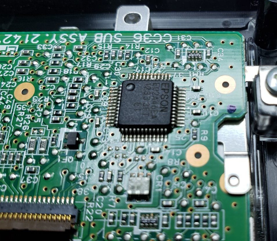
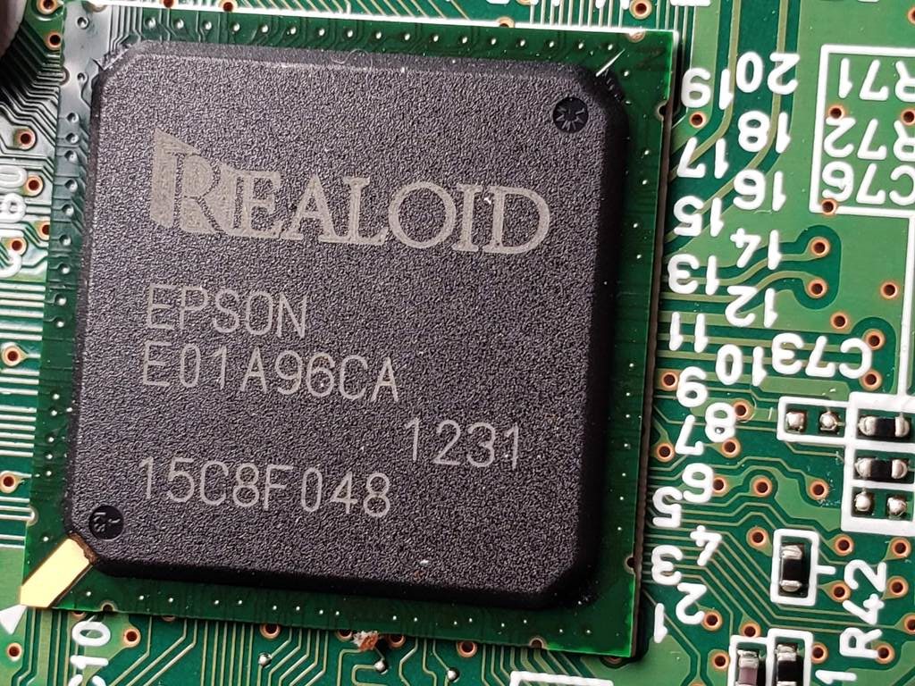
Well, if it isn’t the famous Epson E02A46EA. At last, we meet
Huh. Well, see, the funny thing about Epson is this: they make printers, but they also manufacture semiconductors. They’ve got a whole line of LCD controllers that you can buy, with full support and nicely written datasheets. This isn’t one of them. Search online and you’re not likely to find a datasheet. There might not even be a datasheet. If you’re Epson, and you just need a cheap chip for your own internal use, it doesn’t need a datasheet. It doesn’t need to be flexible enough to operate in hundreds of different applications. It doesn’t even need to make sense. It just needs to work.
This chip works. Maybe there is a complete datasheet floating around at Epson. Maybe there’s just a bunch of post-it notes in some engineer’s cubicle. Either way, it’s unlikely that I’m going to be able to get the necessary documentation. No one outside of Epson knows how this thing works.
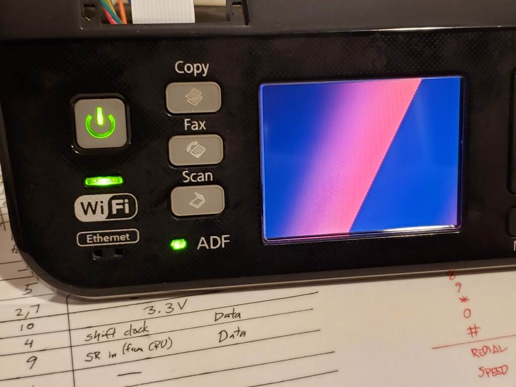
Well, there’s someone. Or something, anyway. But they’re dead. Right?
Doc, I can’t feel my legs. Is it bad?
If it’s alive enough to show me an error screen, it’s alive enough to tell me its secrets. Maybe we can ask nicely. Let’s take a look at the processor! It’s probably a fairly standard–
Oh, come on. Seriously?
“REALOID”. I can only imagine how badly the people who named that wanted to get out of that meeting.
Anyway, suffice it to say we’re not going to learn anything about this processor, so instead we’ll observe what it does. This is where we have to start using more specialized tools. The first stop is an oscilloscope, to see what’s happening on each of the lines that runs to the LCD controller when a video image is being transmitted. I’m not trying to figure out the protocol at this stage; I’m just trying to work out what the pins might be doing.
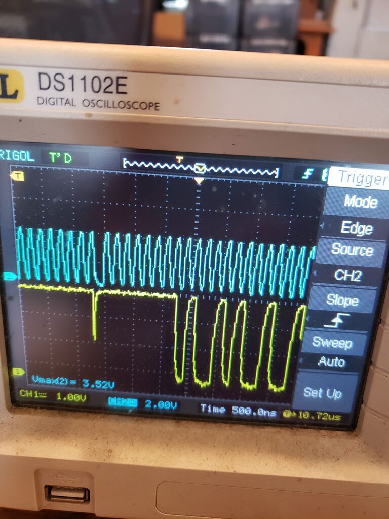
The blue trace in the image above is fairly consistent, so I can presume it’s a clock signal. The more irregular signal in yellow is sending data that’s aligned with the clock. The clock rate here is a steady 6MHz, which is unfortunately pretty close to what our beat-up scope can reliably handle. Probing around, I find that in addition to the clock, I have one line that consistently sends data, another line that goes low for periods of eighteen clocks at a time, and two other lines that also send data, but only when that other line isn’t low. It’s pretty confusing, but between this and my earlier work I can create a spreadsheet of what I think each pin is doing.
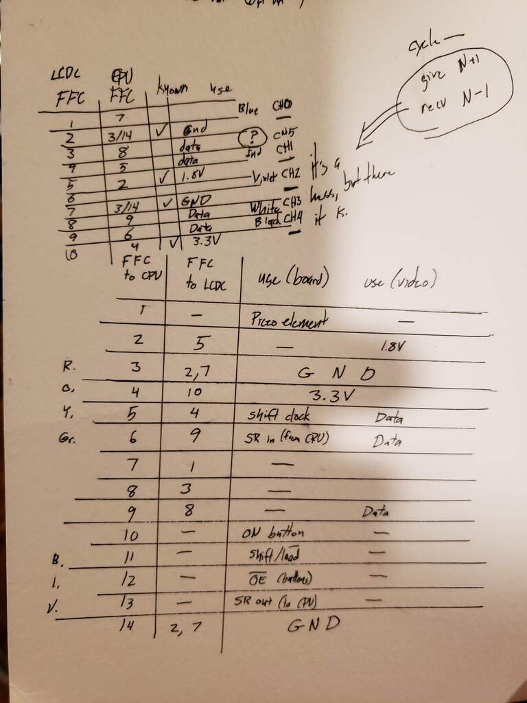
advanced spreadsheet technology
(Around this time I also found a 1.8V line, which powers something on the LCD board. You’ll see a small sub-board in later pictures; that’s the linear regulator I added to generate the 1.8V.)
To figure out the actual data being sent over each line, I hooked up a logic analyzer. I used a first-generation Saleae Logic device (which despite having been discontinued close to a decade ago is still well supported in their latest software– thanks, Saleae!) and sniffed the traffic from the processor to the LCD board. This is what an image frame looks like:
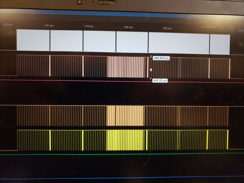
This is the data from the “shutdown” image, which just displays a short message in the middle of an otherwise blank screen. We’re clearly on the right track here, as we’re seeing what we’d expect: a lot of blank space and a burst of interesting data in the middle. You’ll notice that there are “gaps” in the clock signal up top where irregular activity occurs on the data lines. Remember how I mentioned that the buttons and the LCD seemed to be sharing pins? That’s where the processor interrupts sending the image briefly to scan for button presses. The LCD ignores the data pins when it’s not seeing a rising edge on the video clock, so the designers were able to use the same lines for both sets of signals.
Saleae’s software lets you export SPI signals as CSV files, so I exported each of the three data channels separately and then converted them to blobs of binary data. Finally I loaded them up in my old ROM explorer software (which I usually use for finding data in EPROM dumps) and played with the stride length until I found something that looked familiar. And there we go:
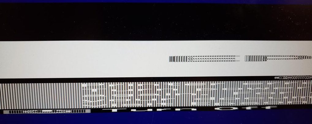
The first thing we notice is how stretched out this image is. Partly this is because I’m viewing individual bits as square pixels, meaning everything is 8x wider than expected, but by counting the length and number of the lines in the image I find that the LCD is receiving 120 lines of 321 pixels each. The final pixel in each line appears to be zero, so I’m guessing these are discarded, and we’re looking at a 320×120 display. The aspect ratio of the screen itself looks more like 4:3, so each pixel on the screen is actually rendered twice as tall as it is wide. The images coming in from the other two data lines are similar, but vary in their bit patterns, indicating that each data line receives data for a different color channel: red, green, or blue.
Then there’s that other line that would go low for groups of eighteen bits at a time. This line indicates to the LCD controller that what’s being sent is a three-byte command, and not image data. There are a bunch of configuration commands sent at startup time, and then one short command (0x31 0x0 0x1) that is sent before every frame of image data. The configuration commands provide the controller with information about how to set up and render images to this specific LCD. We don’t actually care what these commands mean; we only need to record them, and play them back when we start up from a powered-off state.
And that’s about it! At startup we play back the configuration commands, and then try sending a custom image.
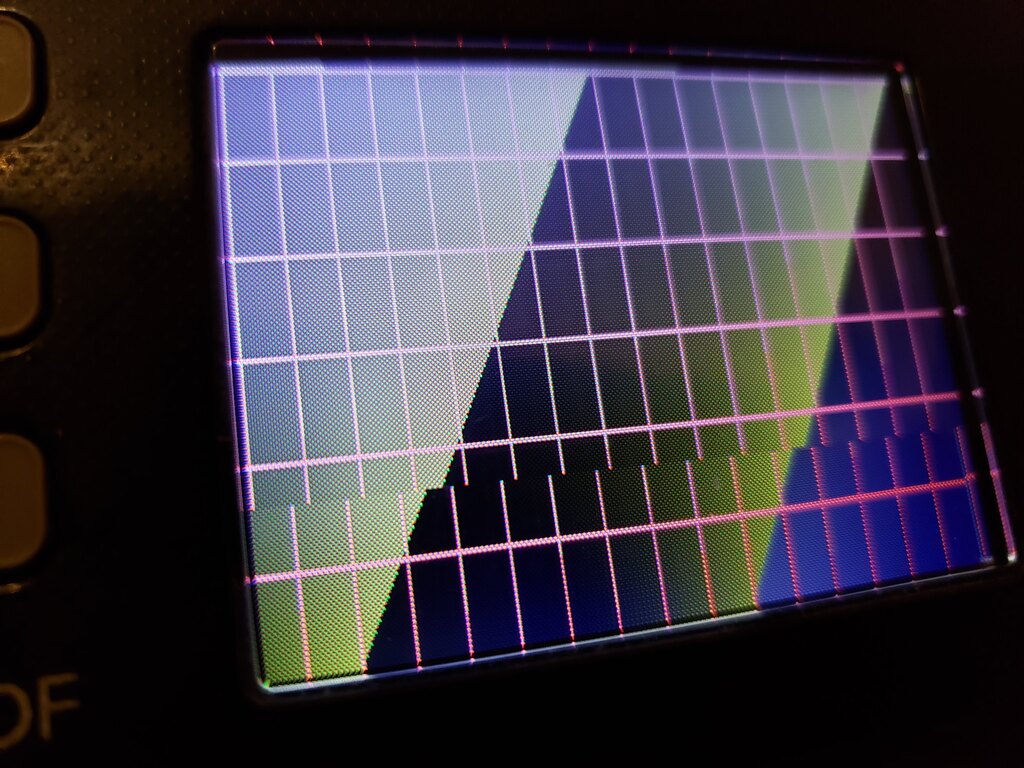
the vaporwave means it’s working
That’s about it for getting the LCD itself working! The rest is optimization and cleanup. I moved the code that sent the actual data to one of the RP2040’s PIO state machines, which can handle shifting data out at a very high rate, and started cranking up the data rate to see what the controller could handle. 6MHz was very stable, and I could get it up to about 10MHz before I started seeing glitches.
You can see the glitching towards the bottom. The horizontal and vertical “lines” are one pixel wide each, and the weird aspect ratio is very apparent.
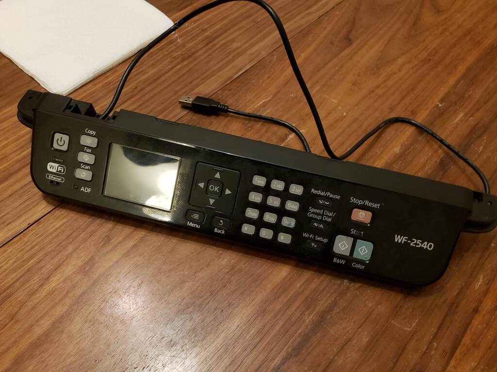
At this point, I’d figured out about everything I needed to know, so I decided to just stuff the Pi Pico itself directly into the case, run a USB cable to the outside world, and call it done for now.
The horrible thing I did before I was done
Since I didn’t need the flat cable connector anymore, I decided I’d just remove it and run wires directly to the pads instead. This was a terrible, terrible mistake.
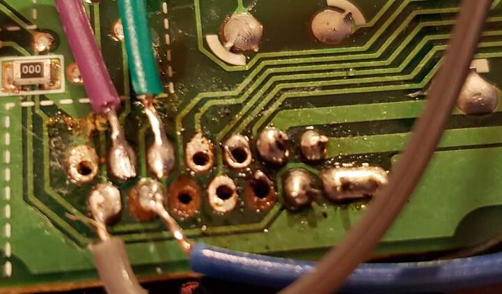
Behold my shame
I’m used to working with double-sided boards, where a through-hole means that there are pads on both sides of the board joined by a plated hole, which is mechanically pretty stable. But this is a single sided board, which means that the pad is only held on to the board by resin on one side. If your iron is set too hot– and mine was– that resin will soften, and the pad will lift off and just disappear. You can see here that I lost a couple of pads while removing the connector. It’s not the end of the world, as there are plenty of other places to solder on a wire, but it was still pretty demoralizing to come this far and then screw this up on the homestretch.
Anyway, I picked myself up, found some thin wire-wrap wire that wouldn’t put too much stress on the pads, and gave it another go.
Could be worse
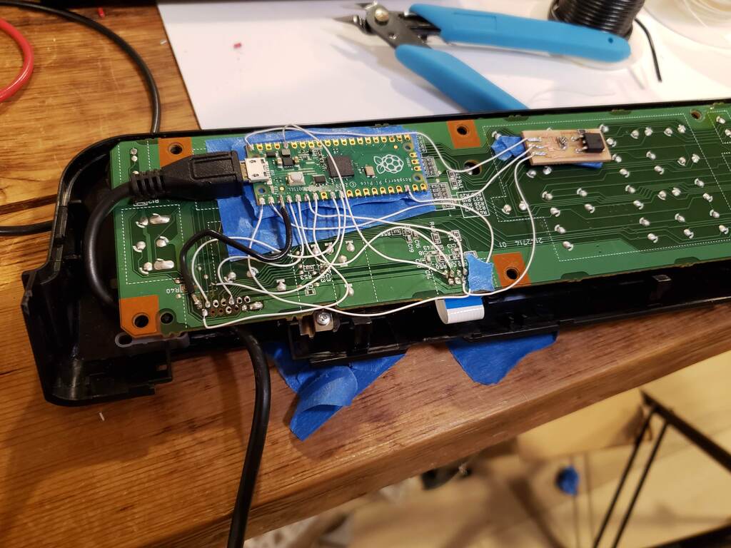
There’s a bit of extra space inside the case, so I used two pieces of painter’s tape and a bit of hot glue to hold the Pi Pico in place on the back of the board. (Nearby you can see that regulator I mentioned earlier.) Where possible, I connected wires to the pins on the LCD controller connector, as that provided a lot of mechanical stability to the pads. Once everything was wired up and tested, I screwed the back panel on and called it a day.
If you want to peek at the code, or read more detailed notes on the LCD controller protocol, feel free to poke around this repository on github.
Now I guess it’s time to start taking apart my toaster.
References
| ↑1 | I’ve also been eating a lot of vindaloo lately. |
|---|
Hello ! Very interesting post, thank you ! I would like to ask you the name of this “Rom explorer software” , which i’m interested for my useful tools collection 🙂
thanks
Dave
Hi Dave,
You can find the rom explorer software at:
https://github.com/nycresistor/romexp
It’s very basic, but I hope you find it useful!
Hackaday brought me here. This was very entertaining, I van’t believe you got that LCD working heh!
Thank you so much for this inspiring guide!
I was able to bring my Epson XP 530 control panel back to life thanks to you, it was so satisfying!
I wrote a library based on yours for those who haven’t thrown away their printers yet: https://github.com/XavierBrassoud/Arduino_Epson_PNL_CE02
Cheers!
Xavier.